"GIANT BOARD™"
ASSEMBLY INSTRUCTIONS
FEATURES:         Cassette I/O
                  System Monitor
                  8 Bit Parallel Input Port
                  8 Bit Parallel Output Port
                  RS232-C/20 MA TTY I/O
                  N Line Decoder For 14 Separate I/O
                  Instruction
|
 |
NETRONICS RESEARCH AND DEVELOPMENT LIMITED
333 LITCHFIELD ROAD (RTE. 202), NEW MILFORD, CONNECTICUT 06776
(203) 354-9375 |
WARNING
Most of the integrated circuits supplied with this kit are of the MOS variety and are, therefore, subject to permanent damage when subjected to any static electricity charges. Static charges may be
present on your body, worktable, or clothing. Even the slightest static may destroy these parts. Do not unpack any of the integrated circuits until you are ready to use them. All MOS integrated
circuits have been carefully tested at the factory prior to shipment. Any integrated circuits returned will be tested, and if evidence of mishandling is detected these parts cannot be replaced free
of charge.
To prepare your self to install MOS integrated circuits we suggest that the following steps be taken. (1) Wrap a piece of bare wire (bell wire with the varnish coating removed will do) around your
wrist. Connect the other end of the wire to ground (a cold water pipe or radiator). (2) Use a sheet of aluminum foil on your work surface, approximately 12" x 15" and ground the aluminum foil to the
same cold water pipe. (3) Make sure that the tip of your soldering iron is grounded. If in doubt re-ground it. (4) Place the printed circuit board and the integrated circuits in their protective
carrier on the aluminum foil work surface. The protective carrier is conductive foam that electrically connects all of the pins of the integrated circuits together, thereby preventing any voltage
drop between the pins.
TOOLS REQUIRED
Low power soldering iron no larger than 35 watts. Preferably lower power with a small pointy grounded tip.
60/40 solder. DO NOT USE additional flux or acid core solder. Use of acid core solder will automatically void all warranties.
Assorted small hand tools, screwdriver, small cutter and needle nose pliers.
PARTS LIST
Check all parts received against the following parts list.
| DESCRIPTION |
|
QUANTITY |
IC 1852                                    2
IC 1853                                    2
IC 74S471 or 18S22N                        1
IC LM3900                                  1
IC 74C02                                   1
IC 40174 or 74C174                         1
IC 74C20                                   1
IC 4050                                    3
IC 4049                                    1
Diode IN4148                               2
Transistor 2N5232 or 2N4384                1
Transistor 2N4355 or 2N5354                2
Capacitor .15uf                            2
Capacitor .015uf                           1
Capacitor .0068uf                          2
Resistor 100 ohm (brown, black, brown)     2
Resistor 390 ohm (orange, white, brown)    1
Resistor 3.9K ohm (orange, white red)      3
Resistor 1K ohm (brown, black, red)        7
Resistor 10K ohm (brown, black, orange)    3
Resistor 22K ohm (red, red, orange)        19
Resistor 100K ohm (brown, black, yellow)   2
Resistor 1 Meg ohm (brown, black, green)   2
|
OPTIONAL PARTS
Connector 86 pin gold plated $5.70 ea.
PRINTED CIRCUIT BOARD ASSEMBLY
( )   1.   Install R2-9, 21, 27, 40 22K resistors (red, red, orange). Solder.

( )   2.   R10-17 22K resistors are bus "pull up" resistors. They are to be used
           on only one of the plug-in boards or on the main motherboard. Check your basic
           ELF and/or other plug-ins. If pull-up resistors have been installed they are not
           required on this board. If you are installing R10-17 on this board remember not
           to install them on subsequent additions. Solder.

( )   3.   Install R18, 24, 33 10K resistors (brown, black orange). Solder.

( )   4.   Install R19, 20 1 Meg resistors (brown, black, green). Solder.

( )   5.   Install R22, 23 100K resistors (brown, black, yellow). Solder.

( )   6.   Install R25, 29, 30, 35, 36, 38, 39 1K resistors (brown, black, red).
           Solder.

( )   7.   Install R31, 32, 37 3.9K resistors (orange, white, red). Solder.

( )   8.   Install R28, 390 ohm resistor (orange, white, brown). Solder.

( )   9.   Install R26 100 ohm resistor (brown, black, brown). Solder.

( )  10.   Install R34 100 ohm resistor (brown, black, brown). Solder. The
           values of this resistor may have to be adjusted to match your terminal
           characteristics and lead lengths.

( )  11.   Install capacitors C1, 4 .15 Mylar. Solder.

( )  12.   Install capacitors C2, 3 .0068 Mylar. Solder.

( )  13.   Install capacitor C5 .015 Mylar. Solder.

( )  14.   Install diodes CR3, 4 1N4148. Note direction. Solder.

( )  15.   Install transistor Q1 2N5232. Solder.

( )  16.   Install transistor Q2, 3 2N4355. Solder.

( )  17.   Install insulated jumpers in board location CR1, 2 as shown. Solder.

( )  18.   Install IC A1 thru A13. Note handling procedure as described on page
           1 Warning.

( )  19.   Install jumpers J1, 3, 8, 9. Solder.
The board is now complete except for jumper selections to be made later.
The Giant Board is designed to plug directly into the ELF II motherboard. Simply install an 86-pin edge connector (Netronics #E86C or equivalent) in the holes provided on the motherboard. Note that
the extreme left bus closest to the edge of the motherboard is reserved for the Giant Board (the 86 pin connector is inserted from the component side). The Giant Board receives its power directly
from the motherboard; the 6.3V transformer should be adequate.
INSTALLING YOUR "GIANT BOARD™"
( )   1.   Install the 86 pin connector. Note this must be installed in the
           extreme left column of holes closest to the left edge of the basic ELF II
           motherboard. Solder.

( )   2.   At this time modifications to your motherboard have to be made. There
           are three slightly different versions depending on the date of purchase
           requiring different modifications to be made. To identify your version, look at
           the area just below IC A14 (adjacent to pins 8-12).
      2a.  If there are no jumpers you have version #1. Proceed to modifications
           for version #1.
      2b.  If there is one jumper labeled J you have version #2. Proceed to
           modifications for version #2.
      2c.  If there are two jumpers labeled J2 and J3 you have version #3.
           Proceed to modifications for version #3.
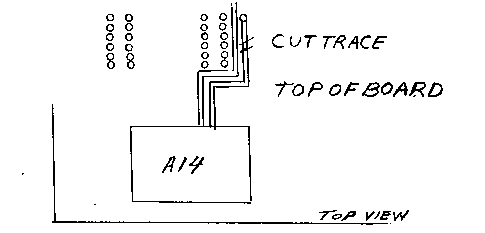
MODIFICATIONS FOR VERSION #1
( )   1.   Cut foil, as shown in Fig A, next to pin 17 of IC A2 (see insert).

( )   2.   Connect pin 17 of IC A2 to bus terminal pin #69 on all bus slots.
           This change enables the first 256 bytes of memory when you are not in the
           monitor program. If you have added a 4K memory and are not using the original
           256 bytes this change is not necessary.

( )   3.   Cut trace, as shown.


( )   4.   Add a wire jumper on the bottom of the board from pin 10 of IC A14 to
           ELF II bus #5 pin 83.

( )   5.   Cut the foil on the bottom of the board between pins 11 and 12 of IC
           A14.

( )   6.   Add a wire jumper on the bottom of the board from pin 11 of IC A14 to
           ELF II bus #5 pin 65.

( )   7.   Remove D9.

( )   8.   Connect a wire jumper from junction of D10 and R26 to ELF II bus #5
           pin 23.

( )   9.   Connect ELF II bus #5 pins 5 and 7 to ground. See Fig. A.

( )  10.   Cut foil on the bottom of the board at trace leaving pin #66 on ELF
           II bus #5. See Fig. A.

( )  11.   The cassette input and output are located one ELF II bus #5 pins 61
           and 59 respectively. Your tape recorder cables can be soldered directly to these
           pins or alternatively pins 61 and 59 can be connected to any unused screw
           terminals. See Fig. A.
MODIFICATIONS FOR VERSION #2
( )   1.   Remove jumper "J" next to IC A2.

( )   2.   Remove jumper "J" below IC A14.

( )   3.   Complete steps 2, 3, 4, 6, 7, 8, 9, 10, 11 listed in modifications
           for version #1.
MODIFICATIONS FOR VERSION #3
( )   1.   Remove J1, 2, 8, 9, 12.

( )   2.   Add jumpers J3, 4, 7, 10, 11.

( )   3.   Remove D9.
PLUGING IN YOUR GIANT BOARD™
( )   1.   Insert the Giant Board into the 86 pin connector. Make sure that the
           component side of the board faces the hex keypad on your ELF II.

( )   2.   Turn on your power supply, check that the output of the LM340T on the
           mother board is producing a ripple free 5 volts (use an oscilloscope, if
           available).
If your power supply voltage is less than 110V AC you may want to increase the size of C-2 on the motherboard; simply add an additional 1000uf on the bottom of the motherboard.
TESTING YOUR GIANT BOARD™
Note once modifications for adding your Giant Board are made, the Giant Board must be in place for proper operation. If the Giant Board is removed pin 17 of A2 must be returned to +5 and D9 must be
reinstalled.
MONITOR TEST (Review Monitor/Editor section)
1.   Set Run, Load ∓ Memory Protect (M/P) off.

2.   Set Load on.

3.   Enter C0, F0, 00, depressing the input button after each byte.

4.   Set load off.

5.   Set Run on.
We are now at the monitor. The C0 instruction is a long branch to F000, the address of the monitor.
Enter:  01;01 should appear on display
        00;00 should appear on display
        00;00 should appear on display
Now depress and hold input button "00" should be on the display. Release the input button and the contents of memory at 0000 should be displayed. This should be C0. Depress and hold the input button
again. 01 should be displayed which is the low-order address of the next memory location to be displayed releasing the input button should reveal the content of this memory location (F0).
Set Run switch off and then back on. We are now back to the beginning of the monitor program at C0 F0 00.
Enter:  02;02 should appear on display
        00;00 should appear on display
        10;10 should appear on display
The Q light should now be on. This means that we will be changing memory starting at 0010
Enter:  7A depress input button, 7A will appear on the display
        3F note that when we depress and hold input button the low-order address of the
           memory to be changed is displayed, which should be 11. When releasing the input
           switch 3F should appear on the display.

Enter:  10
        7B
        30
        11
This is the same program shown in the original ELF II book, but the starting location is now 0010 instead 0f 0000. To run this program starting at 0010 turn the Run switch off then on. Enter 00,
which is the run command to the monitor, then enter 00, 10, the starting address. Depress the input switch again and note that the LED will stay on while the input switch is depressed. Turn Run off
and on again. We are again at the monitor:
Enter:  03 the cassette write command
        00
        00
        00
        FF
Depressing the input switch again should result in the Q light coming on. After 15 seconds the display should start advancing rapidly and stop at FF (the low-order ending address of the data to be
loaded on tape). The Q light will then go out.
The 04 monitor command cannot be tested at this time (see tape test).
The next monitor command to be tested is 05, the search command. Turn the Run switch off and on again.
Enter:  05
        00 Beginning address of search
        10
        7B 00 will be in display
Depress input button again and hold down. The first low-order address containing a 7B will be displayed. This should be a 13. Releasing the input button should reveal the contents 7B. Continuing to
depress and hold the input button will reveal both the low-order address and then the contents of memory.
i.e.    14 depress input
        30 release input
        15 depress input
        11 release input
We will now test the tape recorder function by recording the monitor program on tape and loading the monitor program in the first 256 bytes (0000 to 00FF) of memory. Set Run switch off and return to
on.
Enter:  03 cassette load command
        F0 beginning address to be recorded
        00
        F0 ending address to be recorded
        FF
Make sure that the tape output is connected to the mic input jack on the tape recorder. Start the recorder, allow a few seconds for the tape leader to pass, and then depress the input button. The
display should go to 00 for 15 seconds with the Q light on and then advance to FF. The Q light will go off after the data has been sent out. Rewind the tape and listen to the results. You should hear
a steady tone for 15 seconds then a garbled sound that is the actual data transfer (rewind tape).
Connect the output or remote speaker jack of your tape recorder to the cassette tape input terminal. Set the volume control to mid-position and tone control, if so equipped, to maximum. Go to the
monitor by turning Run off then on.
Enter:  04
        00 beginning address
        00
        00 ending address
        FF
Depress and release the input button again. A "00" should appear on the display. Turn on the tape recorder, after about 15 seconds the display should start advancing to FF and then stop. This would
indicate that the tape has been loaded into memory (0000 to 00FF). If the Q LED comes on before the display advances it would indicate that the output phase of your tape recorder is reversed. Simply
reverse the connectors to the tape input (make sure that the tape output jack is disconnected) and try to load the program again starting by going to the monitor and entering 04, etc. If part of the
program gets loaded and it stops before the display advances to FF try to increase or decrease the volume control. Once making a successful recording (display advances to FF) turn Run off and return
to on. The monitor should be at 000 to 00FF and respond to monitor commands. To test:
Enter:  01
        F0
        00
We should be able to display the contents of the monitor beginning with 90, A1, B3, B4, etc.
IF we had to reverse the tape recorder output to get a successful recording reconnect J2 and disconnect J1 and J3 on the Giant Board. This will reverse the recording phase and allow simultaneous
connection of input and output of your tape recorder.
When exchanging programs with friends try to record their tape. If unsuccessful, reverse speaker leads as before and then load into your memory. Record the program onto your recorder using a new
tape. Reconnect the speaker leads (tape input) and test again.
To test the input, output, and terminal interfaces, suitable I/O devices are required i.e. ASCII keyboard, terminal with RS232 or 20 MA interface, etc. If you decide to use our tiny basic and ASCII
keyboard you will be able to type on the keyboard, displaying the alphanumeric output on your TC screen. You will now be able to run programs in tiny basic, utilizing the full ASCII keyboard instead
of hex keyboard machine language programs.
SYSTEMS MONITOR/EDITOR
The monitor program is stored in ROM IC A10. The address of A10 corresponds to the hex address F0 00 where the most significant four bits of the high-order address are all high. The four-bit latch in
IC A8 decodes these four bits to drive the 4-input NAND gate IC A13. When the F000 address appears the ROM is enabled via pin 16.
To enter the monitor program, turn off the Run, Load and M/P (memory protect) switches to reset the 1802. Place the load switch in the on position and, using the keypad, enter C0 F0 00. Set the load
switch in the off position. When the Run switch is turned on, the monitor will come into play. The next input will determine the monitor mode: 00 is execute, 01 is memory examine, 02 is memory
change, 03 is cassette write, 04 is cassette read, and 05 is memory scan.
To execute (run) a program from a memory location other than 0000, enter the monitor (C0 F0 00), and then enter 00. Insert the two-byte address of the beginning location. When the Input switch
is depressed, the program executes from the memory location specified.
To examine a memory location, enter the monitor and key in 01. Insert the two-byte address of the memory to be examined, then depress and release the Input switch. The byte stored at that
memory location will be displayed. Depress and hold the Input switch down and the low-order address of the next byte is displayed, followed by the memory byte when the Input switch is released.
To change data at a memory location, enter the monitor then enter 02. Insert the two-byte address of the memory to be changed and note that the Q LED comes on. Enter the new data. Then
depress and release the Input switch. The new byte will then be displayed. Note that the low-order address of the next byte is displayed if you hold the Input switch down. If desired, that byte can
also be changed. Loading and checking programs thru the monitor allows easy identification of addresses and corrections.
To cassette write, enter the monitor the enter 03. Key in the starting two-byte address of memory to be recorded, then key in the ending two-byte address. Place the tape recorder in the
record mode, allow several seconds for the leader to pass the heads, and then depress the Input key. The Q LED will extinguish when the recording is complete and the low-order ending address will be
displayed. The tape output of the ELF is connected to the microphone input on your tape recorder.
To cassette read, connect the speaker terminals of your tape recorder to the tape input on the ELF II, enter the monitor and then enter 04. Enter the two-byte address of the memory to be
loaded. Then enter the ending two-byte address. Put the cassette recorder in the playback mode and depress the input switch. Allow 2.5 seconds for each 256 memory bytes recorded. The display will
increment the low-order address of memory being entered. When the display stops incrementing at the last low-order address, the playback is complete. The final digits in the display will show the
low-order address of the data being written (recorded).
To perform a memory scan enter the monitor and then enter 05. Enter the starting address (two-byte) of where you want to begin the search, and then enter the byte that you are searching for;
depress the Input switch twice holding it down the second time. The display will now indicate the first low-order address that the byte appears in memory. Releasing the Input key will then show the
contents of the memory at that location. The monitor is now automatically in the examine mode.
If you are in the monitor program and select an illegal operating code (other than those spelled out above), an EE will be displayed on the readouts and the Q LED will come on.
JUMPER SELECTIONS
You will note that there are a number of jumpers that have not been used. They will be described and utilized in the interconnection instructions to follow. The areas A14, A15, and A16 can be
connected via a 14-wire dip plug soldered directly to the board or via a 14-pin dip socket (not supplied).
8 BIT PARALLEL INPUT CONNECTION
IC A5 is configured to be an 8 bit parallel input port. "Data-in" connections are at pin numbers referenced on the schematic at location A16 on the Giant Board. Data is loaded into the port by an
external device strobe. The negative strobe transition sets the service request to zero (pin 23 of A5). This signal can be connected to either EF3 or INTERRUPT of the 1802. The user has this option
via jumpers J7, J8. We have suggested connecting J8 inasmuch as this is the configuration required for the ASCII keyboard/Tiny Basic. This option allows for an interrupt service routine or software
loop (a 36 instruction, for example, will cause a branch when EF3=0) to respond to the service request that is an input data transfer. Note that pin 23 could be connected to any flag input of the
1802 provided other conflicts in programming and hardware do not exist. The CPU by executing a 6F instruction will enable the input port to the data bus and load M(R(X)) and D with the latched data.
At completion of the 6F instruction execution the service request signal will be reset to 1.
8 BIT PARALLEL OUTPUT CONNECTION
The output port is designed to respond to 1802 program output data transfers. This port, IC A4, has been connected to respond to a 67 instruction. Execution of 67 instructions selects the output
port; the TPB clocks valid data off the data bus into the output port at the proper time. A data ready pulse is available to notify the receiving device that data is available. The output port
connections are available at area A15 on the Giant Board.
It should be noted that any of the instruction signals from the N-Line decoders, IC A1 and A2, could be used and that if additional input and output ports are required they can easily be mounted on
a prototyping board.
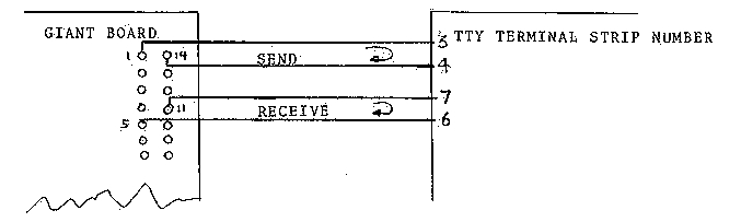
TTY/20 MA INTERFACE
If a 20 MA TTY interface is to be connected, install jumpers J4 and J12. Make sure that J5 and J6 are not installed. The EF4 line, which is the input line to the microprocessor, is shared with the
Input switch on the basic ELF II. The two keyboards cannot be used simultaneously. If you plan to use both, a switch replacing J12 installed either on the Giant Board or at the TTY terminal is
necessary. The inputs and outputs to the TTY terminal are available at area A14 on the Giant Board. Note that your kit has been supplied with R34 at 100 ohms. This value may have to be adjusted
depending on your terminal and/or lead lengths between the terminal and the ELF II. An MA meter in series with the terminal connections should be used to determine the correct value for R34.
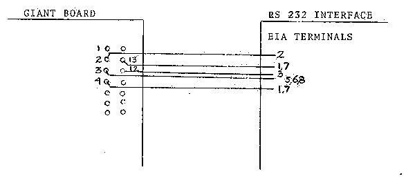
RS232C INTERFACE
To configure the Giant Board for an EIA RS232C interface we must add jumpers J5, J6 and J12. Make sure that J4 is not installed. The EF$ line, which is the input line to the microprocessor, is
shared with the input switch on the basic ELF II. The two keyboards cannot be used simultaneously. If you plan to use both, a switch replacing J12 installed either on the Giant Board or at the
terminal is necessary. The inputs and outputs to the RS232C terminal are available at area A14 on the Giant Board. Note that a -5 to -15V supply voltage is necessary and must be connected to bus #5
pin 15.
N-LINE DECODERS
The Giant Board is equipped with two 1853 3-8 line decoders. They decode the N-Line outputs of the 1802 into 14 separate I/O instructions. IC A1 produces 7 input strobe signals; IC A2 produces 7
output strobe signals. The input and output signals are used to notify an input or output device that it's being asked to perform some function. For example, an output instruction 64 notifies the
9368's, located on the main ELF II, to accept data from the data bus and transfer the data to the dual 7-segment displays. These signals could also be used to turn on and off relays or other devices
with suitable interfacing. Theses signals are brought down to the bus and can conveniently be connected to a prototyping board. Note that a separate decoder for the 64 instruction utilizing IC A6 and
one half of A13 has been included. This was done to ensure compatibility with the original ELF, which requires that the N-Line signal be present from the beginning of the TPA pulse to the end of the
TPB pulse. The 1853 produces this signal only between the trailing edge of TPA and TPB.
SUMMARY OF I/O INSTRUCTIONS USED ON THE ELF SYSTEM
Instruction 61               used to turn TV chip off
Instruction 62               user available
Instruction 63               user available
Instruction 64               used to strobe information on the data bus to dual
                             7-segment display
Instruction 65               user available
Instruction 66               user available
Instruction 67               used to call output port A4 on Giant Board
Instruction 68               not a valid 1802 code
Instruction 69               turns TV chip on
Instruction 6A               user available
Instruction 6B               user available
Instruction 6C               user available
Instruction 6D               user available
Instruction 6E               user available
Instruction 6F               used to call input port IC A5
CASSETTE
Serial data transfer from the processor to a cassette tape utilizes the Q output on the 1802. A program located in the ROM A10 will set and reset the Q producing signals similar to the Kansas City
standard. It is important whether or not your tape recorder inverts the polarity of the output compared to the input signal. This is not important for music, but is extremely important when
transferring data. Most of the machines we have checked do not invert the data. However, we have heard reports that even the same brand may change from run to run. It is largely a function of the
tape head connections. Select the tape recorder that you are going to use and as a trial connect J1 and J3 leaving J2 open. Record the signals as per instructions. If you find that when trying to
load the program from the tape recorder back into memory it does not work, simply reverse the polarity of the input connections and try again. If you can properly load under theses circumstances then
you know that your tape recorder has inverted the signal and you should, at this point, disconnect J1 and J3, and connect J2. This will allow simultaneous connection of both input and output
connections to your tape recorder.
OPTIONAL POWER SUPPLY
Note that your Giant Board has provisions for an on board regulator utilizing an LM340T-5 regulator. This is not required and is made available only for convenience in the event that for some reason
external power is taken from the Giant Board to external circuits. Note this is not required for normal use.
WARRANTY
All of the components supplied in this kit are under warranty for six months from date of purchase. Any parts suspected to be defective should be returned to Netronics with $1.00 for postage and
handling. They will be tested and returned postpaid.
IN CASE OF DIFFICULTY
In the event of difficulty, check all wiring against the instructions. Check for solder bridges and all component values. If you still cannot determine the problem, return the defective printed
circuit board ONLY. Please enclose a check or money order for $7.00 and pack the board securely, and insure the parcel. Your unit will be tested and returned postpaid.
If you suspect a defective component, return the component with $1.00 to cover postage and handling and we will test and return the component prepaid and insured. Mailing address: NETRONICS RESEARCH
& DEVELOPMENT LIMITED, 333 Litchfield Road, Route 202, New Milford, Connecticut 06776, Attention: Service Department.
|
NETRONICS RESEARCH AND DEVELOPMENT LIMITED
333 LITCHFIELD ROAD (RTE. 202), NEW MILFORD, CONNECTICUT 06776
(203) 354-9375 |